Next: Distortion reduction technique Up: Active inductor Previous: Basic characteristics
The active inductor shown in Fig. 4 consists of
a source common transconductor M![]() and a drain common transconductor M
and a drain common transconductor M![]() .
It is obvious that Fig. 4 acts as an active
inductor because a configuration of the active inductor is the same
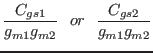
with Fig. 2(a). A gate-to-source parasitic
capacitance of M
.
It is obvious that Fig. 4 acts as an active
inductor because a configuration of the active inductor is the same
with Fig. 2(a). A gate-to-source parasitic
capacitance of M![]() is utilized for
is utilized for ![]() .
.
On the other hand, transconductors used in
Fig. 5 are a source common transconductor M![]() and a gate common transconductor M
and a gate common transconductor M![]() . Bias current of M
. Bias current of M![]() and
M
and
M![]() is shared to reduce its power consumption. The configuration of
Fig. 5 is the same with
Fig. 1(a). Gate-to-source capacitances of M
is shared to reduce its power consumption. The configuration of
Fig. 5 is the same with
Fig. 1(a). Gate-to-source capacitances of M![]() or M
or M![]() is
used as
is
used as ![]() .
.
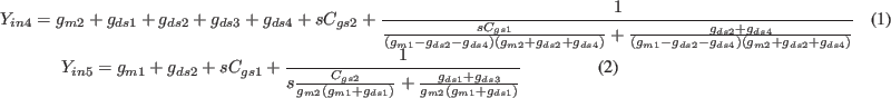
Input admittance of the active inductors shown in
Fig. 4 and Fig. 5 are
shown in Eqs. (4) and (5) respectively.
Because both of Eqs. (4) and (5) can be
represented by
| (5) | |||
| (6) | |||
 |
(7) | ||
 |
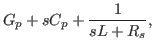
(8) |
Figure 4 requires about twice bias current
compared to Fig. 5. On the other hand, it has
wider input voltage range. Self resonance frequency and ![]() of
Fig. 5 are
of
Fig. 5 are
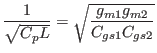 |
(9) | ||
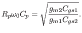 |
(10) |
Takahide Sato 2012-03-31
![\includegraphics[scale=0.65]{active_inductor_new2-2.ps}](img21.png)
![\includegraphics[scale=0.65]{active_inductor3-2.ps}](img22.png)
![\includegraphics[scale=0.65]{active_inductor3-3.ps}](img44.png)